Electron microscopy enables the study of micro and nano-scale structures of materials along with high resolution imaging and elemental analysis. This facility includes equipment for (Scanning) Transmission Electron Microscopy (STEM), Scanning Electron Microscopy/Focused Ion Beam dual beam system (SEM/FIB) and sample preparation.
Facility is open to TRAINED operators 24 hours per day, 7 days per week, and 365 days per year unless the building is closed for maintenance.
The lab is available to RPI Faculty, Students, Staff and external users (on individual basis with review by lab manager and/or director).
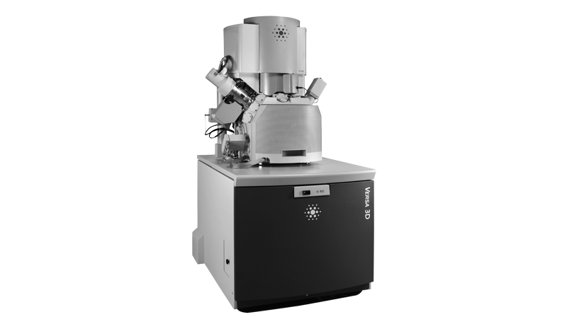
VERSA 3D Duam Beam combines scanning electron microscopy (SEM) and Focused Ion Beam (FIB) in a single platform that allows switching between two modes of operation. The high and low vacuum modes enable users to work with a range of samples including uncoated and non-conductive samples. In addition, the environmental SEM mode allows electron beam imaging of naturally hydrated samples and supports in-situ analysis and visualization at varying temperature and humidity conditions. SEM system provides high resolution imaging with theoretical resolution of 2.3nm while FIB system allows materials manipulation if you are interested in cross-section imaging, Pt-deposition or TEM sample preparation. It is also equipped with EDS system for elemental study and EBSD system for texture/orientation study.
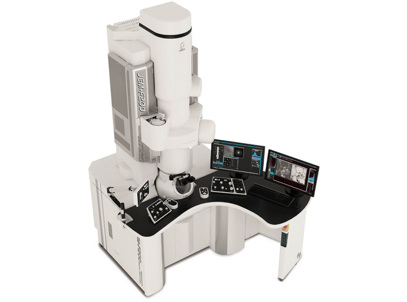
Equipped with cold field emission gun, the JEOL F200 STEM can reach resolution as high as 0.14nm. Gatan Clearview camera with frame rate of 4000 frame per second enable in-situ study. (There are three in-situ holders in the department: heating, bias and liquid/gas holder). It has EDS, EFTEM and EELS system that allow us to study elemental distribution, elemental chemical status, sample thickness, band gap, optical property, polarization property, free electron density, nearest neighbor distribution function, etc. Gatan STEMx control box and continuum camera make 4D STEM, EFTEM/EELS Spectrum imaging possible.
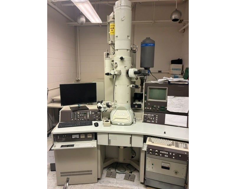
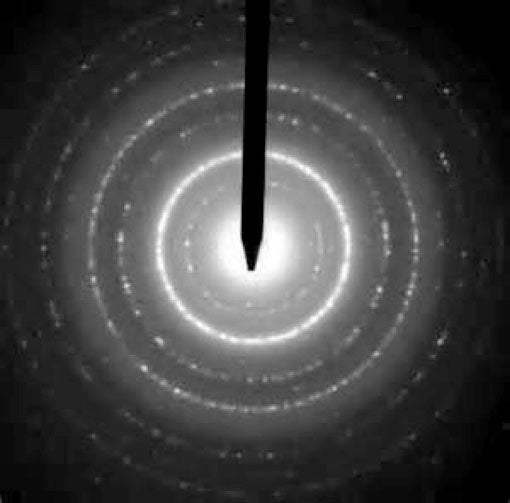
The JEOL JEM-2011 TEM is designed to study the nanostructures and composition of materials through imaging, diffraction, and compositional analysis.
We have variety of sample preparation equipment in the lab, including:
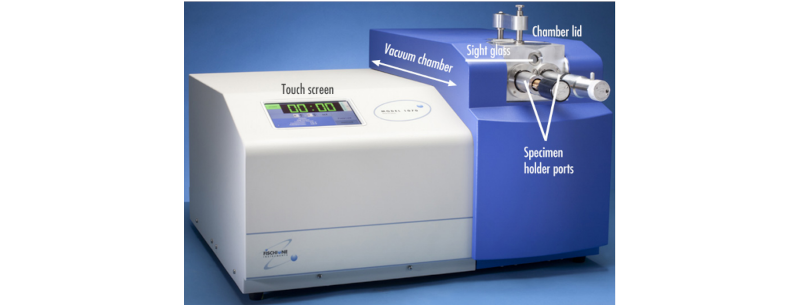
- Fishchione 1070 Nano Clean Plasma Cleaner: for cleaning TEM and SEM samples
- Anatech Sputter Coater: Sputter coater to create a thin metal (Pt) coating for SEM and TEM sample preparation to make sample conductive.
- Carbon Coater: High-vacuum carbon evaporation to create thin and uniform carbon surface coating, down to monolayer.
- Electropolisher: used for TEM sample preparation, highly suitable for metals