

Materials Analysis Laboratories, a part of the Nanoscale Characterization Core (NCC), provide a powerful suite of imaging, spectrometry, and diffraction instruments to interrogate structure, chemistry, and other properties from atomic to micro scales.
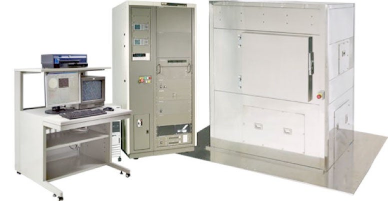
The XPS system provides detailed surface chemistry at the sub-10nm scale. It operates by spectroscopy of photo-electrons emitted from the sample surface by incident X-Ray or ultra-violet photons. These photoelectron energies provide highly sensitive information on chemical species and bonding in the sample surface region. The spatial resolution of this technique is about 10 um, with a spectral resolution of < 0.5 eV. The XPS signal is obtained from regions within about 5-10 nm of the surface, and an integrated ion sputtering enables the surface to be continuously removed, so that chemical depth profiles can be obtained. The system is maintained under ultra-high vacuum (~10-10 Torr) conditions.
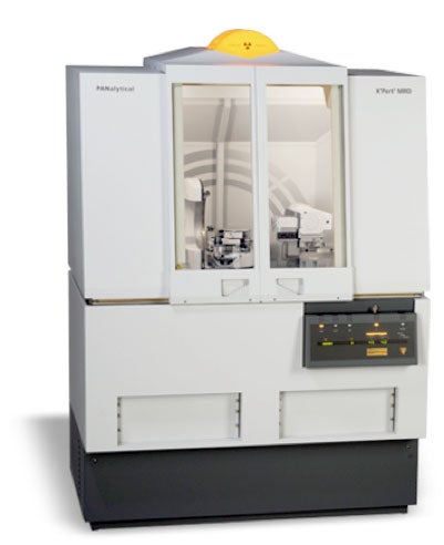
The Panalytical X'Pert Diffractometer is a highly advanced, versatile materials characterization system. The system runs with an open Eulerian cradle (with motorized sample stage enables sample tilts of +/- 90°, in-plane rotation of 360°, in-plane X and Y translations of 100 mm, and vertical Z displacement of 11 mm). Interchangeable PreFIX incident and diffracted beam optics can be configured for optimal measurement of high resolution scans, reflectivity experiments, or for in-plane diffraction. Choice of PreFIX incident beam optics include a graded parabolic x-ray mirror with automatic attenuator, four-bounce Ge(220) monochromator, hybrid four-bounce monochromator with mirror and automatic attenuator, fixed divergence slits, or x-ray lens. High resolution goniometer with optically encoded sample positioning enables a minimum step size of 0.0001°.
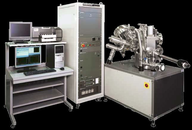
The AES system provides detailed surface chemistry at the sub-10 nm scale. It operates by spectroscopy of Auger electrons (a multi-electron emission process) that are generated by an ultra-fine scanning electron probe. Chemical information from regions as small as 10 nm may be obtained, with chemical sensitivity of a few parts per thousand. The Auger signal is obtained from regions within about 5-10 nm of the surface, and an integrated ion sputtering enables the surface to be continuously removed, so that chemical depth profiles can be obtained. The system is maintained under ultra-high vacuum (~10-10 Torr) conditions.
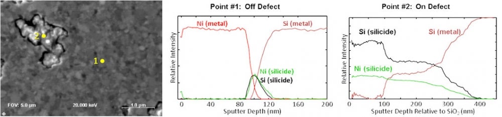 Nanoscale Thin Film Analysis - The sample contains a defect that appeared in a thin nickel film deposited on a silicon substrate after it was annealed to form a nickel silicide at the interface. Multi-point depth profiles obtained with a 20 nm diameter electron beam for analysis and a 500 V Ar ion beam for sputtering were acquired using high energy resolution (0.1%) on and off of the defect.